Technologies
Five process families, one selection discipline
Each page explains what the process does, where it earns its keep and — most importantly — the evaluation dimensions that separate a good tool decision from an expensive one.
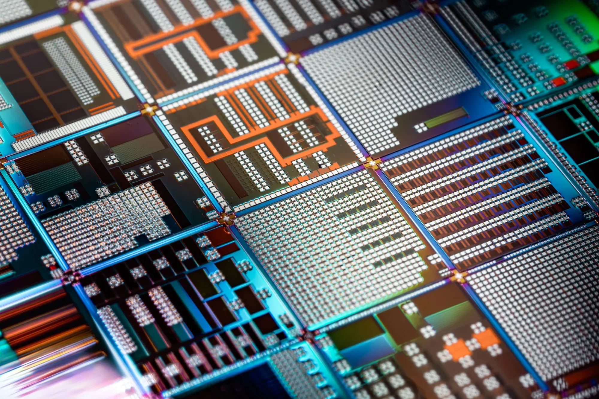
Deep silicon etch (Si DRIE)
Deep reactive ion etching produces the high-aspect-ratio silicon structures behind most MEMS devices, silicon photonics benches and through-silicon vias. It is also the process family where marketing numbers and production reality diverge most easily — which makes disciplined evaluation essential.
Explore this technology
Reactive ion etch (RIE)
RIE and its ICP variants shape the hard and exotic materials that define specialty semiconductors: silicon carbide trenches, GaN mesas, piezoelectric films, optical dielectrics. Each material system rewrites the rules — chemistry, damage behaviour and endpoint discipline all change.
Explore this technology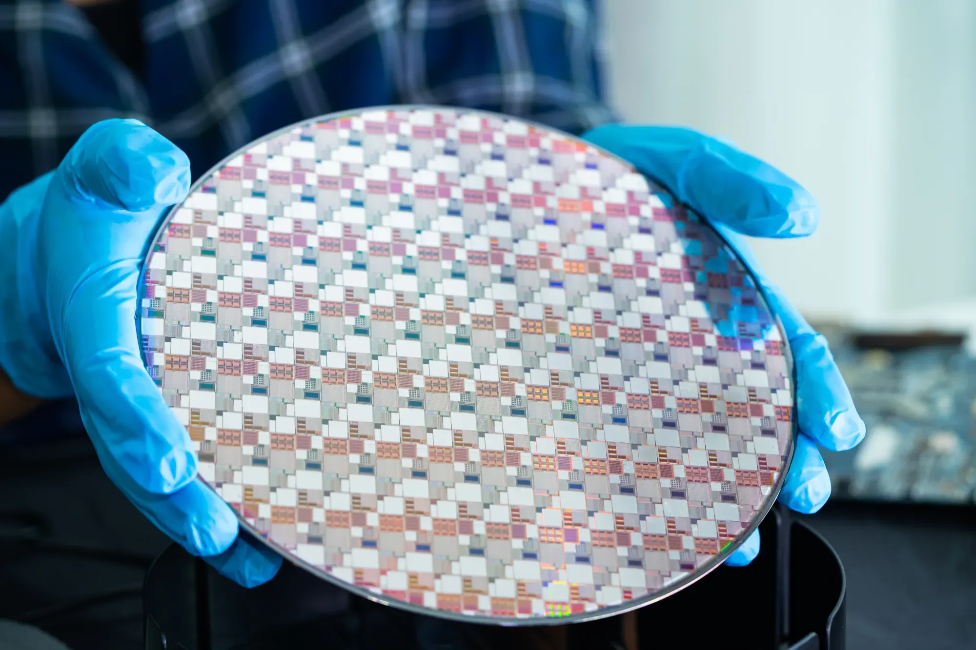
Vapor-phase HF release
The final release etch is where a MEMS wafer carries its highest accumulated value — and where wet processes can destroy it through stiction. Anhydrous vapor-phase HF removes sacrificial oxide dry, freeing structures without the capillary forces of liquid chemistry.
Explore this technology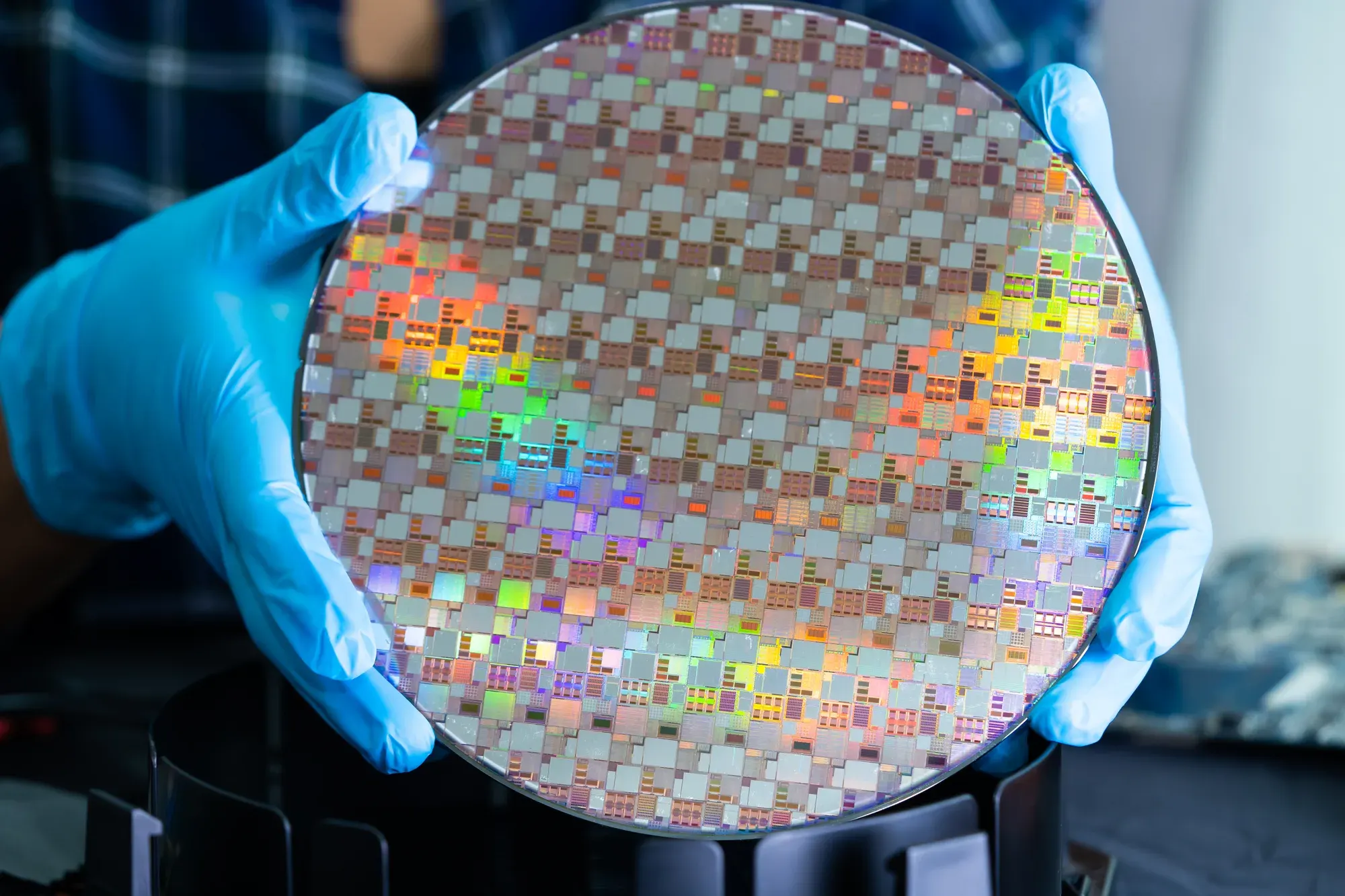
PECVD dielectric deposition
Plasma-enhanced CVD delivers the dielectric films that hold specialty devices together — structural layers, passivation, optical claddings, hard masks — at temperatures the rest of the wafer can survive. Film properties are engineered, not given: stress, composition and uniformity respond to every process knob.
Explore this technology
Batch thermal processing
Oxidation, diffusion, anneal and LPCVD remain the quiet backbone of power-device, sensor and specialty-CMOS flows. Batch furnaces deliver these steps with an economy single-wafer tools cannot match — when temperature uniformity, ambient control and automation fit the application.
Explore this technology
Have a structure, film or thermal step to discuss?
Send a short description of your application — device type, material, wafer size and what a good result looks like. An engineer will reply with a concrete next step.